Skip to content

QUANTARISE · QUANTUM HANDS-ON TRAINING PROGRAM

Hands-on Lithography Training

Step Inside a Real Cleanroom!

Bridging Theory to Practice in Quantum Technologies

Date

14-18 December 2026

Venue

IIT Delhi

Training Mode

In-Person

Organised By

QMD Foundation

About the Program

The QuantaRise: Quantum Hands-on Training Program (QHTP), organised by QMD  Foundation under the National Quantum Mission, connects theoretical knowledge with practical experience in semiconductor fabrication and quantum technologies.

Participants will gain exposure to cleanroom practices, lithography, semiconductor  device processing and electrical characterisation through technical sessions and  laboratory activities at IIT Delhi.

Why This Training Matters

The advancement of quantum technologies depends not only on theoretical breakthroughs but also on the ability to fabricate reliable, scalable, and high-performance semiconductor devices and quantum platforms. Lithography and semiconductor fabrication are fundamental processes for translating quantum concepts into functional devices, enabling the precise patterning, engineering, and integration of materials and device structures at micro and nanoscale dimensions. As India advances its vision through the National Quantum Mission, developing skilled researchers and professionals with practical knowledge of cleanroom protocols, device fabrication, lithography, and electrical characterization is essential for strengthening indigenous capabilities in quantum hardware development. This hands-on training aims to bridge the gap between quantum science and practical device engineering, empowering participants to contribute to the next generation of quantum technologies, semiconductor innovation, and advanced research.
Program Objectives

  • To provide practical, hands on exposure to semiconductor and quantum technologies.
  • To develop experimental and laboratory level skills required for quantum research.
  • To introduce participants to semiconductor device fabrication and cleanroom processes.
  • To strengthen understanding of lithography, device processing, and electrical characterization.
  • To align training activities with national initiatives supported by the National Quantum Mission.

Training Highlights

Cleanroom Exposure

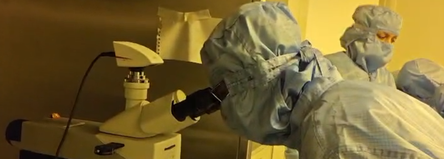
Gain exposure to semiconductor fabrication processes and cleanroom protocols in a real laboratory environment.

Hands-on Lithography

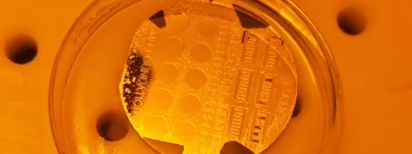
Understand mask design, device layout, patterning, and maskless photolithography.

Semiconductor Device Fabrication

Learn essential fabrication processes, including wafer cleaning, metallization, contact formation, and lift-off.

Device Characterization

Get introduced to electrical characterization techniques, including I–V measurements and Hall-effect measurements.

Data Analysis and Interpretation

Understand device measurement results and their interpretation.

Expert-Led Technical Sessions

Interact with researchers and experts working in semiconductor and quantum technologies.

What You Will Learn

  • Introduction to National Quantum Mission
  • Fundamentals of Quantum Technologies
  • Quantum Materials and Quantum-Enabled Semiconductor Devices
  • Cleanroom Protocols
  • Material Growth Techniques for Quantum Devices
  • Introduction to CMOS Technology
  • Quantum Device Structures (FETs and Junctions)
  • Wafer Cleaning
  • Mask Design and Device Layout
  • Oxide Film Deposition/Growth
  • Maskless Photolithography
  • Contact Formation and Lift-off
  • Electrical Characterization (I–V and Hall Effect)
  • Electrical Measurements Using Probe Systems
  • Data Analysis and Interpretation
  • Research Opportunities and National Quantum Mission Proposals

Training Schedule

Day 1

  • Inauguration and Introduction to the National Quantum Mission
  • Fundamentals of Quantum Technologies
  • Cleanroom Protocols
  • Visit to the Cleanroom Facility

Day 2

  • Material Growth Techniques for Quantum Devices
  • Introduction to CMOS Technology
  • Wafer Cleaning
  • Mask Design and Device Layout

Day 3

  • Device Structures (FETs and Junctions)
  • Oxide Film Deposition/Growth
  • Maskless Photolithography

Day 4

  • Electrical Characterization (I–V and Hall Effect)
  • Maskless Photolithography
  • Contact Formation and Lift-off

Day 5

  • Data Analysis and Interpretation
  • Electrical Measurements Using Probe Systems
  • Research Opportunities and National Quantum Mission Proposals
  • Interaction with Speakers and Participants
  • Valedictory Session and Certificate Distribution 

Who Can Apply?

  • B.Tech Students
  • M.Tech Students
  • M.Sc. Students
  • Ph.D. Scholars
  • Scientists
  • Startups
  • Industry Professionals
  • Postdoctoral Researchers

Registration Fee

B.Tech / M.Tech / M.Sc. Students

₹5,000

Ph.D./ Post Doc. Students / Scientists

₹15,000

Startups / Industry Professionals

₹15,000

Important: Please select the appropriate participant category while completing the registration form.
*Shortlisted candidates will be notified with payment instructions.

Facilities and Training

Glimpses of Previous Programs

Frequently Asked Questions

What is the duration of the training program?

The program is conducted over 5 days.

The offline training sessions will be conducted at IIT Delhi.

B.Tech, M.Tech, M.Sc., and Ph.D. students, postdoctoral researchers, scientists, startups, and industry professionals can apply.

The registration fee is ₹10,000 for B.Tech/M.Tech/M.Sc./Ph.D. students, ₹15,000 for postdoctoral researchers/scientists, and ₹20,000 for startups/industry professionals.

Yes. Certificate distribution is scheduled during the valedictory session on the final day.

Yes. The offline component includes exposure to cleanroom facilities and practical semiconductor fabrication and characterization activities.

Participants can register through the online registration link available on this webpage.

Register for the Program.

Interested candidates can register through the online registration portal.
Step 1: Click on the Register Now button.
Step 2: Fill in the required personal, academic, and professional details.
Step 3: Select your participant category.
Step 4: Complete the registration fee payment as instructed.
Step 5: Submit the registration form and wait for confirmation.

← Back

Thank you for your response. ✨

Current Course(required)

Drag and drop or click to select a file.

Drag and drop or click to select a file.